


Understanding graphene
Graphene is a single layer (monolayer) of carbon atoms, tightly bound in a hexagonal honeycomb lattice. It is an allotrope of carbon in the form of a plane of sp2-bonded atoms with a molecular bond length of 0.142 nanometres. Layers of graphene stacked on top of each other form graphite, with an interplanar spacing of 0.335 nanometres. The separate layers of graphene in graphite are held together by van der Waals forces, which can be overcome during exfoliation of graphene from graphite.
Graphene is the thinnest compound known to man at one atom thick, the lightest material known (with 1 square meter weighing around 0.77 milligrams), the strongest compound discovered (between 100-300 times stronger than steel with a tensile strength of 130 GPa and a Young's modulus of 1 TPa - 150,000,000 psi), the best conductor of heat at room temperature (at (4.84±0.44) × 10^3 to (5.30±0.48) × 10^3 W·m−1·K−1) and also the best conductor of electricity known (studies have shown electron mobility at values of more than 200,000 cm2·V−1·s−1). Other notable properties of graphene are its uniform absorption of light across the visible and near-infrared parts of the spectrum (πα ≈ 2.3%), and its potential suitability for use in spin transport.
Bearing this in mind, one might be surprised to know that carbon is the second most abundant mass within the human body and the fourth most abundant element in the universe (by mass), after hydrogen, helium and oxygen. This makes carbon the chemical basis for all known life on earth, making graphene potentially an eco-friendly, sustainable solution for an almost limitless number of applications. Since the discovery (or more accurately, the mechanical obtainment) of graphene, applications within different scientific disciplines have exploded, with huge gains being made particularly in high-frequency electronics, bio, chemical and magnetic sensors, ultra-wide bandwidth photodetectors, and energy storage and generation.
Graphene production challenges
Initially, the only method of making large-area graphene was a very expensive and complex process (of chemical vapour deposition, CVD) that involved the use of toxic chemicals to grow graphene as a monolayer by exposing Platinum, Nickel or Titanium Carbide to ethylene or benzene at high temperatures. There were no alternatives of using crystalline epitaxy on anything other than a metallic substrate. These production issues made graphene initially unavailable for developmental research and commercial uses. Also, using the CVD graphene in electronics was hindered by the difficulty of removing the graphene layers from the metallic substrate without damaging the graphene.
However, studies in 2012 found that by analysing graphene’s interfacial adhesive energy, it is possible to effectively separate graphene from the metallic board on which it is grown, whilst also being able to reuse the board for future applications theoretically an infinite number of times, therefore reducing the toxic waste previously created in this process. Furthermore, the quality of the graphene that was separated by using this method was sufficiently high to create molecular electronic devices.

Research in growing CVD graphene has since progressed by the leaps, rendering the quality of graphene a non-issue to technological adoption, which is now governed by the cost of the underlying metal substrate. Nevertheless, research is still being undertaken to consistently produce graphene on custom substrates with control over impurities such as ripples, doping levels and domain size, whilst also controlling the number and relative crystallographic orientation of the graphene layers.
Applications
Driving graphene research towards industrial applications requires coordinated efforts, such as the billion-euro EU project Graphene Flagship. After the first phase that lasted several years, Flagship researchers produced a refined graphene applications roadmap, that pinpoints the most promising application areas: composites, energy, telecommunications, electronics, sensors and imaging, and biomedical technologies.
Being able to create supercapacitors out of graphene will possibly be the largest step in electronic engineering in a long time. While the development of electronic components has been progressing at a very high rate over the last 20 years, power storage solutions such as batteries and capacitors have been the primary limiting factor due to size, power capacity and efficiency (most types of batteries are very inefficient, and capacitors are even less so). For example lithium-ion batteries face a trade-off between energy density and power density.
In initial tests carried out, laser-scribed graphene (LSG) supercapacitors demonstrated power density comparable to that of high-power lithium-ion batteries that are in use today. Not only that, but also LSG supercapacitors are highly flexible, light, quick to charge, thin, and as previously mentioned comparably very inexpensive to produce.
"The possibilities of what we can achieve with the materials and knowledge we have, have been blown wide open"
Graphene is also being used to boost not only the capacity and charge rate of batteries but also the longevity. Currently, while such materials as lithium are able to store large amounts of energy, that potential amount diminishes on every charge or recharge due to electrode wear. With graphene tin oxide as an anode in lithium ion batteries for example, batteries last much longer between charges (potential capacity has increased by a factor of 10), and with almost no reduction in storage capacity between charges, effectively making technology such as electronically powered vehicles a much more viable transport solution in the future. This means that batteries (or capacitors) can be developed to last much longer and at higher capacities than previously realized. Also, it means that electronic devices may be charged within seconds, rather than minutes or hours and have hugely improved longevity.

Researchers in the Graphene Flagship are also looking into ways that graphene can be used to improve energy generation, including the improvement of perovskite solar cells (PSCs), highly promising next-generation solar power sources with very high efficiency. Flagship researchers made excellent progress in improving the lifetime and performance of PSCs, while reducing the production cost of PSCs. Adding a reduced graphene oxide spacer layer to a PSC resulted in low-cost production of PSCs with 20% efficiency, retained up to 95% after 1000h of operation. A pilot production line and a 1 kW graphene-perovskite solar farm are in the pipeline for the next period.
The usage of graphene in energy storage is most notably researched through the use of graphene in advanced electrodes. Combining graphene and silicon nanoparticles resulted in anodes that maintain 92% of their energy capacity over 300 charge-discharge cycles, with a high maximum capacity of 1500 mAh per gram of silicon. Achieved energy density values are well above 400 Wh/kg. In the next Flagship phase, a Spearhead project will focus on pre-industrial production of a silicon-graphene-based lithium ion battery. Furthermore, a spray-coating deposition tool for graphene was developed , enabling large-scale production of thin films of graphene which were used, for example, to produce supercapacitors with very high power densities.
Another use for graphene along similar lines to those mentioned previously is that in paint. Graphene is highly inert and so can act as a corrosion barrier between oxygen and water diffusion. This could mean that future vehicles could be made to be corrosion resistant as graphene can be made to be grown onto any metal surface (given the right conditions). Due to its strength, graphene is also currently being developed as a potential replacement for Kevlar in protective clothing, and will eventually be seen in vehicle manufacture and possibly even used as a building material.
Graphene has long been regarded as an ideal candidate channel material for radio frequency (RF) flexible electronics. Radio frequency and even terahertz applications are constantly being pushed forward, with a demonstrated microwave receiver for signals up to 2.45 GHz, a flexible THz detector, and a demonstration of efficient cooling of graphene-based nanoelectronic devices using hyperbolic phonon cooling. The flexible nature of graphene allows for various electronic devices on flexible substrates, such as for example flexible, all-solid-state graphene-based supercapacitors, wearable touch panels, strain sensors, and self-powered triboelectric sensors, all recently demonstrated, with applications such as fiexible, robust touschscreen devices such as mobile devices and wrist watches closely on the horizon.
Beyond these near-term applications, one could expect foldable televisions and telephones and eventually electronic flexible newspapers containing publications of interest that can be updated via wireless data transfer. Graphene being extremely transparent it is expected to be a component of intelligent (and extremely durable) windows in homes, with (potentially) virtual curtains or content display ability.
Optical communication formed the backbone of the internet age and is expected to be equally pivotal for the developing 5G networks. Modern communications rely on optical links that fly information at the speed of light, and on circuitry such as photodetectors and modulators which is able to encode a wealth of information onto these light beams. Although silicon is the material of choice for photonic waveguides on optical chips, photodetectors are made from other semiconductors such as GaAs, InP, or GaN, because silicon is transparent at standard telecomm wavelengths. Integrating these other semiconductors with silicon is difficult, complicating fabrication processes and raising expenses. Also, thermal management is becoming a problem as photonic devices keep shrinking while using more power.
Graphene is a promising material for telecomm photodetectors, because it absorbs light over a large bandwidth, including standard telecomm wavelengths. It is also compatible with CMOS technology, which means it can be technologically integrated with silicon photonics. Furthermore, graphene is an excellent heat conductor, promising a reduction in heat consumption of graphene-based photonic devices. For these reasons, graphene for optical communications has been an intense field of research, which is now gaining fruition in full working prototypes.
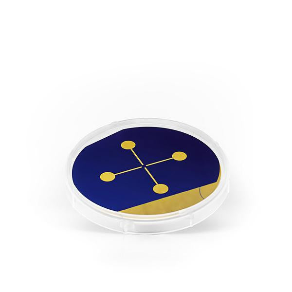
In 2016, the bandwidth of graphene photodetectors reached 65 GHz, utilizing graphene/silicon pn junctions with potential bit rates of ~90 Gbit s-1. Already in 2017, graphene photodetectors with a bandwidth exceeding 75 GHz were fabricated in a 6” wafer process line. These record-breaking devices were showcased at the Mobile World Congress in Barcelona in 2018, where visitors could experience the world’s first all-graphene optical communication link operating at a data rate of 25 Gbit s-1 per channel. In this demonstration, all active electro-optic operations were performed on graphene devices. A graphene modulator processed the data on the transmitter side of the network, encoding an electronic data stream to an optical signal. On the receiver side, a graphene photodetector did the opposite, converting the optical modulation into an electronic signal. The devices were made with Graphenea CVD graphene and showcased at the Graphene Pavilion.
Graphene produced with chemical vapor deposition (CVD) will form the cornerstone of future graphene-based chemical, biological, and other types of sensors. The 2D nature of the material provides intrinsic advantages for sensing applications, because the entire material volume acts as a sensing surface. Furthermore, graphene provides excellent mechanical strength, thermal and electrical conductivity, compactness, and potentially low cost, which is necessary for competing on the crowded sensor market.
Graphene-based gas/vapor sensors have attracted much attention in recent years due to their variety of structures, unique sensing performance, room-temperature working conditions, and tremendous application prospects. Apart from water vapor, graphene has been used to sense gases such as NH3, NO2, H2, CO, SO2, H2S, as well as vapor of volatile organic compounds, resulting in a dramatic rise in scientific publication numbers on this topic. Graphene has also been used to detect traces of opioids in concentrations as low as 10 picograms per milliliter of liquid.
This multitude of favorable properties has led to a wide array of investigations into graphene use for biosensing. Particularly interesting configurations are graphene field-effect transistors (GFETs) and graphene enhanced surface plasmon resonance (SPR). These types of graphene sensors have been used for DNA, protein, glucose, and bacteria detection. Using GFET, biosensors with a detection limit of 10 pg/mL were produced for opioid molecules.
Graphene is also an enabling technology for novel, flexible magnetic field sensors. The market for magnetic field sensors is an expanding one, with size estimates up to USD 4.16 billion in 2022. The multiple purposes of magnetic field sensors such as position detection, current monitoring, speed detection, and angular sensing allow access to a wide range of industries such as automotive, consumer electronics, healthcare and defense. A most common magnetic sensor type utilizes the Hall effect, the production of a potential difference across an electrical conductor when a magnetic field is applied.
The key factor for determining sensitivity of Hall effect sensors is high electron mobility. As such, graphene is a highly interesting material for this application, with measured carrier mobility in excess of 200,000 cm2 V-1 s-1. Graphene Hall sensors with current-related sensitivity up to 5700 V/AT and voltage-related sensitivity up to 3 V/VT were demonstrated in graphene encapsulated in boron nitride. Such performance outpaces state-of-the-art silicon and III/V Halls sensors, with a magnetic resolution as low as 50 nT/√Hz. The current practical limit for sensitivity of graphene Halls devices on industry standard wafers is around ~3000 V/AT. For comparison, state of the art Hall sensors from traditional CMOS-compatible materials have sensitivity on the order of ~100 V/AT. Even flexible graphene Hall sensors, produced on Kapton tape, reach sensitivities similar to rigid silicon Hall sensors.
Combining some of these aforementioned potential uses, one can imagine visionary applications such as car security systems that are connected to the paint on the vehicle - not only would a car alarm be able to tell if someone is touching the vehicle, it would be able to record that information and send it to the owner's smartphone in real time. Such "smart paint" could also be used to analyze vehicle accidents to determine initial contact patches and resultant consequential energy dispersion.
The market will soon see clothing containing graphene-enhanced photovoltaic cells and supercapacitors, meaning that we will be able to charge our mobile telephones and tablet computers in a matter of minutes (potentially even seconds) whilst walking to school or work. We may possibly even see security-orientated clothing offering protection against unwanted contact with the use of electrical discharge.
Game changer
In summary, this discovery by a physics professor and his PhD student in a laboratory in Manchester, where they used a piece of graphite and some Scotch tape has completely revolutionized the way we look at potential limits of our abilities as scientists, engineers and inventors. The possibilities of what we can achieve with the materials and knowledge we have, have been blown wide open, and it is now conceivable to imagine such amazing prospective situations as lightning fast, yet super-small computers, invisibility cloaks, smart phones that last weeks between charges, and computers that we can fold up and carry in our pockets wherever we go.
View Our Graphene Products / Read More Graphene Publications / Contact Us


