Graphene and quantum dot IR sensors for food quality
Food quality and health is a growing concern in a world with increasing population, with markets for food safety and quality testing predicted to grow by percentages in the double digits (CAGR) over the next decade. Personal low-cost sensors, ideally integrated into smartphone cameras, are becoming proliferous as the capabilities of those cameras expand. Graphenea and ICFO are working on the GRAQDOBLEA project, funded by the Ministry of Industry and Competitiveness of Spain program Retos Colaboracion 2016 (RTC-2016-5505-2) to develop graphene sensors for food quality monitoring. These low-cost high-performance sensors will operate both in the infrared (IR) and visible range of the light spectrum, accessing a spectral region that is particularly sensitive to fruit bruising, for example. In addition, when performing as a multiband spectrometer, the sensor can reveal compound structure information for organic and biological compounds. The graphene sensor overcomes the technological thresholds of other competing technologies for broadband detection, such as Silicon, InGaAs, T2SL, and InSb (that operate in narrow spectral ranges) or HgCdTe (that has a high cost).
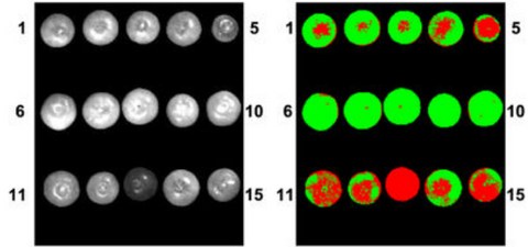
Figure: IR imaging and classification of healthy and bruised tissue in blueberries (Sci. Rep. 6, 35679 (2016)). Red is bruised, green is healthy.
The sensor is built based on the technology of hybrid graphene/quantum dot photodetectors developed at ICFO. The unique properties of graphene, such as its high charge carrier mobility, charge carrier density and a large mean free path, enable a high photoconductive gain (105 or higher). Tunable carrier density in graphene allows optimization of charge recollection and device efficiency. The usage of quantum dots as light absorbers enables easy deposition over rigid and flexible substrates and an absorption of light over a broad wavelength range. These high-gain, low noise, broadband sensors have shown to have extraordinary performance in a CMOS camera configuration and are developed using the same process as for conventional silicon fabrication technology and monolithic integration. Aside from being used for food monitoring purposes, this type of photosensor and camera could also be used for night vision (automotive), biomedical, process inspection, safety and surveillance, crop inspection, among other applications.
The goal of the joint project is to provide proof of principle for the technology at wafer scale (200mm). A particular challenge on the project will involve increasing pixel density from the current 384x288p to 1920x1080p, aiming for a pixel size of 3 micrometers. A material development challenge is to ensure wafer scale uniformity and controlled doping for uniform performance across one chip and equal functionality of all chips on a wafer. The duration of the project is three years and it is funded by the "Retos de Colaboracion" program of the Ministry of Economy and Competitiveness of Spain, which aims at facilitating the public-private collaborations in the development of new products.

