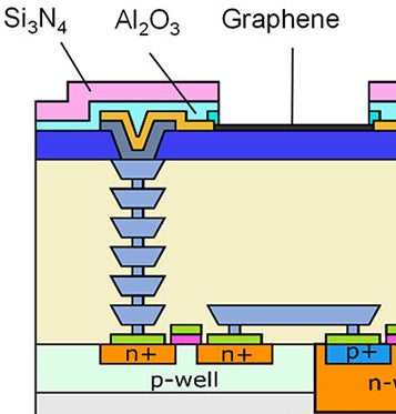
Graphenea and the WOW-2D Consortium: Pioneering Wafer-Scale Integra...

San Sebastián, Spain — The global semiconductor industry is undergoing a massive transformation, shifting from traditional silicon manufa...

Read story

Graphenea and the WOW-2D Consortium: Pioneering Wafer-Scale Integration for 2D Optoelectronics

Wafer-scale CMOS-integrated graphene field-effect transistor arrays...

Researchers report wafer-scale fabrication of CMOS-integrated graphene-field effect transistor (GFET) arrays with extremely high yield an...

Read story

Wafer-scale CMOS-integrated graphene field-effect transistor arrays for biosensing

Graphenea receives government officials as part of PERTE effort

On Dec 20th, Graphenea in its headquarters in San Sebastian received two government officials who visited the company offices, cleanroom,...

Read story

Graphenea receives government officials as part of PERTE effort

Multilab characterization towards standardized graphene

Characterizing the properties of graphene in a standardized manner is a prerequisite to industrial adoption of the material. Although Ram...

Read story

Multilab characterization towards standardized graphene

Graphenea’s Cartridge S2X makes sensing easy

Graphenea has released a new product to make sensing with graphene easy for every customer. Introducing the Cartridge S2X, a package that...

Read story

Graphenea’s Cartridge S2X makes sensing easy

Tags