High-frequency graphene transistors enabled by contact engineering
High-frequency performance of graphene field-effect transistors (GFETs) has been improved with a reduced resistance between the graphene and engineered metal contacts. A research team from Italy, Spain, and the USA has successfully reduced contact resistance below 50 W mm which is required for high-frequency applications. The high-frequency performance of the GFETs was confirmed by exhibiting transconductance as high as 940 S/m.
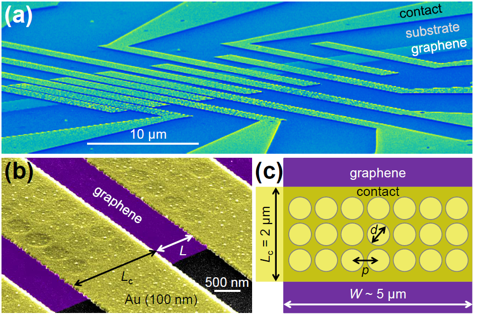
Figure: Engineered metal contacts reduce contact resistance to GFETs, enabling high-frequency performance (Luca Anzi et al 2018 2D Mater. in press https://doi.org/10.1088/2053-1583/aaab96)
Graphene has long been regarded as attractive for applications in high-frequency electronics, due to its large carrier mobility and saturation velocity. However, conventional (ohmic) contacts between graphene and various metals exhibit rather large contact resistance (Rc ~ 500 W mm), significantly reducing the mobility of contacted graphene and preventing it from reaching its true potential in high-frequency applications. Contact resistance below 50 W mm is desired and is a typical value in high-frequency transistors.
Various strategies have been adopted to reduce contact resistance in GFETs, including engineering contact geometry to maximize charge injection through graphene edges and minimize injection through the surface. Graphene edges have a high density of states, which allows for efficient injection of charges from the metal contact into the GFET. The most recent solution utilizes arrays of circular holes in the graphene sheet below the metal contacts, which brings the contact resistance down to just 23 W mm with gold contacts. In contrast to previous studies, this work achieves such low contact resistance at the Dirac point of graphene, where the carrier density is low. Operation near the Dirac point has several advantages, including access to physical phenomena that occur close to the Dirac point, and enabling cascading of different transistor stages for multi-stage circuits.
These “holey” contacts outperform standard contacts from various tested metals, such as Au, Pd/Au, Ni/Au, Ag, Au/Al, and Ni/Al. This most recent research, published in the journal 2D Materials, together with the proliferation of high-quality wafer-scale graphene, clears the path for use of GFETs in high-frequency electronics.
