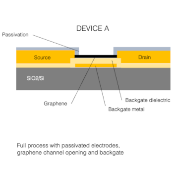
Posted by Marko Spasenovic on April 17, 2013 0 Comments
Water purification and desalination is one of the great challenges of mankind, with 1.1 billion people living without proper drinking water. In particular, portable water purifiers and filters are always in demand, and new technologies are being sought to lower the cost and energy footprint. Nanotechnology holds great potential for getting rid of bacteria and other harmful contaminants, and now graphene water filters are showing great potential.
Graphene sheets perforated by small holes have first been explored by researchers at MIT as potential candidates for water filtration. Holes with a diameter of 1 nanometer (a billionth of a meter) are big enough to let water molecules sift through, however small enough to stop any undesired chemicals. The news of MIT's discovery was so big that the Smithsonian magazine, the publication of the famous Smithsonian Institution, named it one of the top 5 surprising scientific milestones of 2012, along with the Higgs Boson, the discovery of Earth-like planets, and NASA’s Curiosity mission to Mars.
Whereas only one year ago nanometer-sized holes in graphene sheets sounded like a pipe dream, recent months brought news of actual graphene nanopore devices, with various uses such as DNA detectors or traps to study small numbers of silicon atoms. With graphene sheet nanopores a reality, a graphene water filter comes within reach.
Top-notch scientific researchers are not the only ones toying with the idea of solving the world's problems with graphene. Lockheed Martin, the famous weapon manufacturer, recently announced that it has obtained a patent for graphene nanopore-based water filters. The technology, called Perforene, is similar to that studied at MIT. A prototype is expected by the end of the year.
As with a few other high-tech applications of graphene, the technology for mass production has not yet been reached. However, with the likes of Lockheed Martin investing in the graphene nanomanufacturing, solutions are expected in the near future. The current results are very promising - graphene, due to its small weight and size, could significantly reduce the costs and energy footprint of portable water filters and desalinators.
Posted by Marko Spasenovic on April 03, 2013 0 Comments
Team Graphenea has once again worked in
close collaboration with research scientists and published another
high-impact scientific paper. Our most recent publication, in last
month's edition of Nature Physics, shows multiplication of electrons after light absorption by graphene. The work may prove important for future graphene-based solar cells. Amaia Zurutuza, Amaia Pesquera and Alba Centeno made the graphene for our collaborators at ICFO (Barcelona), MIT, and the Max Planck Institute for polymer physics.
Graphene absorbs light of all colors,
ranging from the ultraviolet to far infrared. When graphene absorbs a
photon, which is a particle of light, a conducting electron is
created in the graphene. The electron is free to move and carry
electricity. Such a photoabsorption process is the key process in
solar cells and photodetectors.
Together with the world-renowned groups
of Koppens (ICFO), Levitov (MIT), and Bonn (Max Planck) we have shown that conducting
electrons in graphene multiply as they move, producing more
conducting electrons. Essentially, instead of losing energy to heat the
graphene crystal, which is what would happen in most other materials,
in graphene the electrons give their energy to promote other
electrons to the conduction band.
The project is a show of Graphenea's wide multinational scientific collaboration. The experiment was designed at ICFO in Barcelona, carried out at Amsterdam and Mainz (Max Planck), and the experimental findings explained in detail with the help of theoretical physicists from MIT. Graphenea remains the supplier of choice for high quality graphene to scientists worldwide.
It's not the first time that Graphenea publishes high level scientific papers. Last year, our graphene was featured in Nature, when we showed that graphene can support surface plasmons, essentially guiding light waves along the graphene sheet. In that case we also collaborated with the Koppens group, as well as with the group of Hillenbrand here at nanoGune, the parent institute that spun off Graphenea.
"We at Graphenea work to provide the best materials for the research community and the industry", says Jesus de la Fuente, our CEO. "Our close collaboration with research scientists at the cutting edge continues to bear fruit for both sides".
We currently have three products available from Sigma-Aldrich:
Monolayer graphene film on SiO2/Si substrate, product number 773700
Monolayer graphene film on copper foil, product number 773697
Monolayer graphene film on quartz, product number 773719
About Sigma-Aldrich: Sigma-Aldrich is a leading Life Science and High Technology company whose biochemical, organic chemical products, kits and services are used in scientific research, including genomic and proteomic research, biotechnology, pharmaceutical development, the diagnosis of disease and as key components in pharmaceutical, diagnostics and high technology manufacturing. Sigma-Aldrich customers include more than 1.3 million scientists and technologists in life science companies, university and government institutions, hospitals and industry. The Company operates in 38 countries and has nearly 9,000 employees whose objective is to provide excellent service worldwide. Sigma-Aldrich is committed to accelerating customer success through innovation and leadership in Life Science and High Technology.
Posted by Jean-Christophe Lavocat on January 28, 2013 6 Comments
The development of graphene has a very high pace. The production of graphene is made in different ways, for instance by chemical vapor deposition or by growth on Si, and the applications and quality vary a lot. In this blog post we will try to help you deciding which kind of graphene is good for a given application. We will also introduce you to the ratio price/quality that has a real importance for mass scale production.
Properties of graphene
Selecting graphene for a given device (flexible book, sensor, lab on chip, you name it) is a choice based on its outstanding properties. Not every device would benefit from these features of course, but it is amazing to see the number of fields where graphene outperfoms other standard materials.
Property
Graphene
Electron mobility (at room temperature)
2,5 x 105 cm2 V-1 s-1
Young's Modulus
1TPa
High thermal conductivity
> 3000 WmK-1
Optical absorption
3,00%
In addition to that, graphene is impermeable to any gases can sustain high densities of electric current.
These values are for very high quality graphene. In reality, most graphene types will come close to these numbers, so depending on your application you would like to use very pure forms of graphene or not.
Different types of graphene
Liquid phase and thermal exfoliation
Liquid phase and thermal exfoliation is a process in which graphite is exposed to solvents or a thermal shock that will allow the splitting of individual graphene flakes. Despite mass production is already reached, during this process several layers are created, and sometimes impurities are inserted in the flakes. One can also collect smaller platelets of graphene by using nanotubes instead of graphite but the process are longer and more expensive.
Synthesis on Silicon Carbide
Silicon Carbide is a widely used material in the field of electronics. By sublimating the atoms of Si, the remaining face of the SiC has a graphite surface. Nowadays the number of layers of graphene could be controlled and the quality is very high over a wide area (crystallites of some hundreds of micrometers ). Drawbacks are the high cost of SiC and the high temperatures required to produce the sublimation. The two factors will probably confine SiC graphene to niche markets like high-frequency transistors or metrology resistance standards.
Chemical Vapor Deposition
CVD represents nowadays the easiest process to prepare high quality graphene in large amount. After evaporation of carbon atoms on a copper foil, the method allows transfer of graphene to a broad range of substrates. For instance it can be transfered to silicon waffers were nano sized electronics can be designed. CVD graphene does not contain many defects ( grain boundaries or inclusion of thicker layers are common but not critical).
The quality over price ratio already allows CVD graphene to be used for many applications like transparent and flexible electronics. Also, since graphene is an efficient gas barrier, it is used as an anti-corrosion coating.
Other types
Other types of graphene exist, like mechanical exfoliation of molecular assembly, but there use is very limited. Indeed, with mechanical exfolliation, for istance, you can only produce small flakes. The interest is bounded to the academic level for very specific experiments.The same limitation occurs with molecular assembly for instance.
Applications of Graphene
Graphene could be used in various fields like sensors and metrology, biotechnology, high-frequency transistors, flexible and transparent electronics, batteries or photonics. For most of these areas, CVD graphene is the best candidate in terms of cost and quality. However, few of them could require special fabrication methods. Nanoelectronics for example could be done more easily with molecular assembly of graphene. Graphene ink or graphene paint that could be used into printed electronics could be fabricated with liquid phase exfoliation.
You have an application but you are not sure about the technology you need? Tell us on our forums. We will be here to answer you.
To know more :
Novoselov KS, Fal'ko VI, Colombo L, Gellert PR, Schwab MG, & Kim K (2012). A roadmap for graphene. Nature, 490 (7419), 192-200 PMID: 23060189
Posted by Jean-Christophe Lavocat on January 16, 2013 2 Comments
Graphene Live is a serie of conferences where material providers, equipment makers, policymakers industrials, investors and academics meet and speak about the market of graphene. Several topics are presented, from the applications, to the technology developments through the appearance of new market sectors. The last episode was held last December in Santa Clara, California, USA and visitors from more than 30 countries where attending the conference.
Tradeshow Graphene and printed electronics
In addition to the different talks, a tradeshow was combined between an other event about Printed Electronics. It was a perfect place to meet partners in graphene if you work in the printed electronics area. For instance, Novacentrix, Heraeus Precious Metals, Roth & Rau or Thin Film Electronics were exhibiting there.
A « demonstration street » had also been prepared with the latest technology in printed flexible displays such as posters, e-readers, audio paper, interactive games, OLED displays, electronics in fabrics, interactive printed controls and menus, printed RFID and much more.
Conference about graphene
Graphene Live was definetely the hotest place to hear about graphene last year : 4 keynotes, 5 talks about touch screen and replacement for ITO, two presentations about manufacturing and equipment and many more on various applications such as sensors, quantum materials or energy storage with graphene.
Graphenea was happy to attend the conference, and our Scientific Director, Amaia Zurutuza, gave a presentation about synthesis, transfer, characterization and potential applications of graphene in an industrial context. Her dedicated work here in Spain has already lead to the publication of a Nature article as well as a patent filed.
Graphene Live Europe
The next event will be hosted in Europe, in Berlin (Germany). Be sure to save the date (April 17th and 18th, 2013) since Jesus De La Fuente, Graphenea's CEO, will be there to give a presentation. The two days will follow the same organization as the one from the USA. If you are an investor, an electronics manufacturer or just a graphene curious, come and meet us there. We will be happy to discuss with you.
What was the last conference about graphene that you attended? Did you like it or not? Drop a line of comment below to start the discussion.
Posted by Jean-Christophe Lavocat on December 24, 2012 0 Comments
From November 25 to November 30, Graphenea was attending the Material Research Society (MRS) Fall Meeting in Boston. This meeting intend to gather the top scientists and companies working for better materials.
MRS Presentation
The MRS was founded in 1973 and is an organization opened to academia, industry and government material researchers. The Society promotes all kind of actions related to this interdisciplinary field. Members of the Society help to communicate about the progress of material science. Today, 16,000 members are registered over more than 70 countries. The Society is different from that of single discipline professional societies because it encourages communication and technical information exchange across the various fields of science affecting materials.
In addition to exchange within the Society by the mean of publications and symposium proceedings (MRS Bulletin and Journal of Material Research), MRS sponsors two major annual Meetings offering approximately 95 topical symposia. The Society push forward the interaction among professionals and students through University Chapters.
Symposium on Carbon Nanomaterial
This year, Graphenea have been sponsoring the Symposium on Carbon Nanomaterial. A large amount of presentations were made to describe the progress in graphene research. Among those, Graphenea have been particularly interested in CVD graphene :
Controlling Orientation, Edge Geometry and Thickness of High Quality Large-area CVD Graphene - Presented by Nicole Grobert from Department of Materials, University of Oxford
Combinatorial Methods for Wafer-scale CVD Graphene Synthesis - Presented by Jeremy Cheng from Intermolecular Inc. (http://www.intermolecular.com), San Jose, California, USA
Gas Transport Control in Graphene Growth by Chemical Vapor Deposition on Copper Foil - Presented by Seong-Yong Cho from Department of Materials Science and Engineering, Seoul National University, Seoul, Republic of Korea
Activation Energy Paths for Graphene Nucleation and Growth on Cu - Presented by Cecilia Mattevi from Imperial College London, London, United Kingdom
Study on Interface between Graphene Domains Grown by Ambient-pressure CVD - Presented by Yui Ogawa from Kyushu University, Fukuoka, Japan
Optical and Electrical Characterization of CVD Graphene Transferred to SiO2/Si Substrates for Biosensor Applications - Presented by Flavio Plentz from Physics, UFMG, Belo Horizonte, MG, Brazil
Correlation of Carrier Diffusion and Defect Structure in CVD-grown Graphene - Presented by Caitlin Rochford from Sandia National Laboratories, Albuquerque, New Mexico, USA
As you know, Graphenea is deeply involved in research and development of graphene, as well as industrial applications. Since most commercial application requires high quality and high reproducibility, we produce Chemical Vapor Deposited Graphene. If you like that topic, you can register to our mailing list to receive all the most recent news.
Posted by Jean-Christophe Lavocat on December 25, 2012 1 Comment
Not such a long time ago, say five to six years, people were still using wide and heavy cell phones. They were only able to do one thing : to give a phone call. Nowadays, the technology enabled smart phones : they are able to browse the web, to be your personal assistant, you play games with them, and you even record movies or take photos that could be instantly uploaded on Facebook or Tweeter. What a revolution !
However progress is a never ending story. You cannot spend a week without discovering some new high tech device. In the world of graphene, this is happening at a very impressive pace. One good thing with graphene, is that its applications are never far from the public's attention. Remember our article about graphene enhancing batteries' lifetime ? Cellphone and tablets producers are already thinking about graphene to improve their devices.
Graphene enables flexible phones
In a word, when you use graphene, electronics becomes smaller and flat. Since it becomes possible to build very thin, transparent and flexible electrodes, many industry sectors will embrace the technology. For instance we produce graphene for Nokia and they are planning on releasing a flexible phone soon. We have already presented the project of flexible display sooner this year. This time Nokia goes further and enters the race of flexible phones. At the moment, no precise date is given by Nokia or any other electronic firm. However, Nokia released a video clip showing the possibility of such a phone. It is quite amazing to think ten years in the past, and compare this phone with the famous N3310 for example.
In the video you can appreciate the flexibility and the transparency of the device. All that is due to graphene electrodes. Here at Graphenea we are very impatient to see this kind of phone on the market. What about you?
Posted by Jean-Christophe Lavocat on December 12, 2012 2 Comments
The famous US aerospace and aeronautics agency NASA is currently developing sensors based on graphene. The main leader of the
initiative, Mahmooda Sultana, joined NASA's Goddard Space Flight
Center in Greenbelt two years ago. She had since then won research
and development fundings to install graphene production facilities.
NASA's graphene production
is based on Chemical Vapor Deposition a technique widely spread among
the microelectronics industry. The same material, also known as CVD
graphene, is developed in our
labs at Graphenea.
Sultana's group is now
manufacturing high quality graphene and is working on applications.
For them, the most promising use of graphene is with chemical
sensors.
Chemical sensors based
on graphene
The original vision
of tiny instruments for atmosphere sensing is due to Fred Herrero who
has been pushing NASA's research line in that direction for over a
decade now. The encounter between Sultana and Fred gave birth to the development of a miniaturized, low-mass, low-power, graphene-based
detector. The aim of this device is top measure the amount of
single-atom oxygen in the upper atmosphere.
Researchers already know
that atomic oxygen accounts for up to 96 percent of the low Earth
atmosphere that creates the atmospheric drag experienced by orbiting
spacecrafts. This atmospheric drag leads to a premature loss of
altitude for the satellites.
"We still don’t know the impact
of atomic elements on spacecraft in creating a drag force," he
said.
"We don’t know how much momentum is transferred between the
atom and the spacecraft. This is important because engineers need to
understand the impact to estimate the lifetime of a spacecraft and
how long it will take before the spacecraft reenters Earth’s
atmosphere."
The solution came
naturally from graphene and Sultana's expertise. Like many metals,
when graphene absorbs an ato of oxygen, a change of electrical
resistance occurs. The advantage of graphene is that it greatly
simplifies the steps needed to measure atomic oxygen. Sultana also
claims a similar chemical sensor could be used for methane, carbon
monoxide or other kind of gases. However she admits that her research
is still at an early stage.
Strain Detection
An other useful graphene
application for NASA would be the detection of stress in engineered
composites. By embedding stress-sensitive graphene in a multi-layer
composite, they can obtain smart material that could monitor internal
stress.
For that purpose, NASA is
collaborating with the MIT (where Sultana studied as a PhD student).
They plan to produce large sheets of CVD graphene to be deployed in a
non invasive way to detect damage or potential source of breakage.
Replacing the relatively large instruments currently in use for
strain detection with thin and light graphene-based devices would be
a great step forward.
“We can employ a
different combination of its extreme properties and use the same
material for different sensing applications,” Sultana says. “That’s
the beauty of graphene.”
To know more : Li, Mary; Sultana, Mahmooda; Hess, Larry (2012). Graphene Transparent Conductive Electrodes for Next- Generation Microshutter Arrays NASA Tech Briefs, May 2012 Other: 20120009225
Posted by Jean-Christophe Lavocat on November 29, 2012 0 Comments
In 2005, when Andre Geim and Philip Kim separately worked on graphene's electrons and showed that the material was showing a zero-bandgap, this came as a very curious feature that people would probably use. This zero-bandgap property makes that graphene is not a real semi-conductor and could not be used directly by the industry. Many successful attempts were made to create a band gap in graphene, by using doped graphene, nanoribbons or by using an electric field between a bi-layered graphene.
Few would have thought about bending graphene to get a band gap. However, this idea has been followed by Edward Conrad since three years now in Georgia Tech. He has been working on graphene grown on surfaces with small grooves (18 nanometers deep). When graphene is deposited over these trenches a semiconducting behavior appears. The results were published this month in the journal Nature physics and show a 0.5 electonvolts band gap.
We asked Edward Conrad some questions about his last publication :
How did you get the idea to study graphene's conduction on a topological
surface? Did you have any feelings about the result beforehand?
E. Conrad : Our group has been working on sidewall growth techniques for the last three years. The
goal was to get around lithography defined ribbons that have very rough edges and
therefore can not lead to semiconducting graphene. In the process developed at
Georgia Tech we grow graphene on the walls of shallow trenches etched into Silicon carbide (SiC) that leads to
very narrow ribbons. We have been developing arrays of these ribbons that are so
well ordered that we can measure their electronic band structure using angle
resolved photoemission. Our intent was to show directly that the graphene on the sidewalls was
semiconducting.
After two years of work with no success, a wider set of data scans
showed that the curved part of the the graphene, as it bends over the trench edge,
becomes semiconducting. This was a big surprise to us! We did not expect the bend
to have any significant gap. This is a classical example of how experimental
physics runs down a path and finds a new turn in the road that was unexpected.
Has your research been inspired by some other previous work?
E. Conrad : We had no idea that this bent graphene would be such a good
semiconductor. There has been theory work on strained graphene, but nothing I am
aware suggest such a gap.
Can you give us some details about the growing of the graphene on your
surface? Do you think that introducing trenches on the waffer can become
critical in the deposition of graphene?
E. Conrad : Graphene grows ordered on Silicon Carbide. You heat the SiC in a carbon furnace and graphene
grows. It has a specific orientation relative to the SiC atomic lattice. There was
early work that showed graphene grows over atomic steps in SiC.
What we did was to
patterned ordered arrays of steps in the SiC with know depth and orientation rather
than rely on random steps that occur on the blank SiC wafers. The fact that
graphene grows so ordered on SiC allowed us to make more than 10,000 parallel
trenches and thus 10,000 graphene ribbons. This allowed us to have a system where
we could measure the band structure of ribbons as small as 1.4nm wide.
Graphene grown on SiC trenches (left) - Photoemission
spectroscopy (right)
Most people measure the band structure indirectly through resistance
measurements. The problem with that method is that dirt, disorder, width variations
all make the interpretation of these experiments difficult. Using our ordered
system, we can measure the band structure, and therefore the gap, directly.
What are the direct applications you see in this result?
E. Conrad : Making high speed low power transistors out of graphene has always been the goal.
Without a band gap this could never happen and graphene would never compete with Si
transistors. We are currently trying to build a Schottky barrier transistor out of
this material. If it works, it will open up a scalable way to make all carbon
integrated circuits.
What could be industrial constraints about these applications?
E. Conrad : Thinking about industrial constraints at this point is a bad idea. First we must
prove the device will work, then we worry about how to build them on an industrial
scale. The example is the invention of the transistor. They built the first
transistor out of germanium (Ge), one of the most expensive materials know at the time
(only ~20 people ever held the stuff). When they found out Ge transistors did not
work well enough they started a project to build it out of an even more expensive
material that no one knew how to purify: silicon.
The point is, if the device has
properties compelling enough the engineering will follow. In this case graphene can
in principle operate at switching speeds much higher than silicon and does not have the
same heating problems. If the device we are building works well enough, graphene
high speed devices will start to enter the market.
How long have you been working on that project?
E. Conrad : I started working on graphene soon after the original patent for graphene
electronics were submitted by Georgia Tech in 2001 (4 years before the work that led
to a Nobel prize). By the way, the noble prize for graphene
was given for its discovery in 2004 even though graphene was known to exist as early
as 1960s and rediscovered again in the 1980s and 1990s.
What do you think about the media coverage about graphene?
E. Conrad : There is way too much media coverage. A lot of hype about future electronics when a
band gap (step one in electronics) has never been shown to exist until now. There
is a lot of serious work left to be done to prove that graphene electronics is
feasible. Research is slow and methodical.
People who make predictions should not always be listened too.
If you want to follow news about graphene we suggest you to register to the mailing list and follow us on Twitter or Google+.
To know more : Hicks, J., Tejeda, A., Taleb-Ibrahimi, A., Nevius, M., Wang, F., Shepperd, K., Palmer, J., Bertran, F., Le Fèvre, P., Kunc, J., de Heer, W., Berger, C., & Conrad, E. (2012). A wide-bandgap metal–semiconductor–metal nanostructure made entirely from graphene Nature Physics DOI: 10.1038/nphys2487
Posted by Jean-Christophe Lavocat on November 20, 2012 0 Comments
If you are a frequent user of smartphone or tablet, you know more than others that "mobility" is a magic word. However, when was the last time your iPad was plugged to recharge its battery? Probably less than 24 hours ago. What if graphene was providing the world with a disruptive technology allowing batteries to last three times longer? This is what California Lithium Battery, a start-up based in Los Angeles, is aiming for.
Despite the obvious mobile phones/tablets market, this is not the main target of this young company. The two major sectors that California Lithium Battery wants to conquer is the one of electric vehicles and the less known grid storage facilities.
Environmental-friendly focused research
Prof. Harold Kung is principal investigator of a technology that was detailed one year ago. As a researcher at Northwestern University, he was trying to develop an effective way to increase battery life. He and his team started looking into Si–Graphene composite five years ago and was focused on reducing carbon emission from vehicles.
I looked into why people don’t like to buy electric cars, which is because of the battery life. So looking into that, we said 'What can we do about it?' Improve energy density and power delivery.
Harold Kung
The result did not come long after that. Instead of using the classical graphite at the anode of their battery, the team used Si-Graphene, a layered material containing Silicon and Graphene. The idea was published in October 2011 in the journal "Advanced Energy Materials".
From the lab to the market
Just one year after this, the company California Lithium Battery, led by Phil Roberts, collaborated with Argonne National Laboratory and announced an important milestone for the new technology. The new type of anode, called GEN3, which contains SI-Graphene and is used with advanced cathode and electrolyte materials, increases energy density by 3 times and specific anode capacity by 4 times over existing lithium-ion batteries (LIBs). They claim that :
Independent full cell tests reveal performance characteristics, with an energy density of 525WH/Kg and specific anode capacity 1,250mAh/g. In contrast, most commercial LIBs have an energy density of between 100-180WH/kg and a specific anode capacity of 325mAh/g. This equates to more than a 300% improvement in LIB capacity and an estimated 70% reduction in lifetime cost for batteries.
Phil Roberts
The company plans to produce industrially the new GEN3 within two years. Phil Roberts, the CEO, thinks that they will replace graphite anodes in most lithium batteries over the next 2-3 years.
Graphene in your cars, mobile phones and laptops
If the technology hits its target, LIBs could be produced for under $175/kWh (135€/kWh) and compete with the cost of fossil-fuelled powered vehicles. The car industry is currently looking for an efficient energy storage technology to reduce both costs and weight, but also improve lifetime.
However the first daily life objects that would benefit from the graphene-based battery are probably portable electronics. Despite the fact Kung is not directly involved in the company, he is currently filling a patent of one variant of the technology. He is in talks with cell phone companies to commercialize his own graphene-based battery.
The pace at which graphene came out from the lab to the front row of advanced technology is quite unusual. Discovered in 2004 it won the Nobel prize in 2010, and people already think of using it in mobile devices no later than in 2014. So just 10 years after its discovery. Here at Graphenea we believe that a revolution is occurring now and we help other companies to work with the best graphene products. That's what we are aiming for, and that's what we do.
If you want to follow news about graphene we suggest you to register to the mailing list and follow us on Twitter or Google+.
Tell us what kind of graphene you need and we will produce it for you. Our knowledge and equipment mean almost any need can be met and on any scale - research, pilot line and industrial. To discuss your customised graphene requirements, provide your details using the...