


Written By: Miklos Bolza
Graphene has been revolutionizing electronics since October 2004 when Andre Geim and Kostya Novoselov first determined how to remove a single layer of carbon lattice from graphite. The production and research of today’s graphene field effect transistors (GFETs) would not have been possible without the past two decades of research, and offer many benefits over traditional bipolar junction transistors. This is all thanks to the inherent qualities of graphene, which means GFETs can be used to good effect in a range of technologies, including biological and chemical sensors.
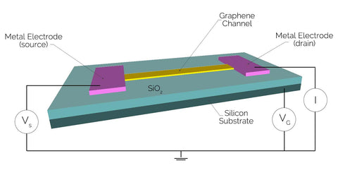
Understanding Field Effect Transistors
A field effect transistor (FET) is an electrical component which uses a nearby electric field and its associated voltage differential to modulate the current flow. FETs are generally devices with three terminals, or electrodes: a semiconductor channel runs between two of these electrodes – the source and the drain – while a third, called the gate, acts as the control. The voltage differential applied to the gate allows or blocks the charge transport through the semiconductor channel depending on its direction and strength.

Structure of GFETs
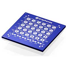
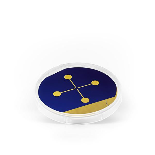
Graphene field-effect transistors (GFETs) take the typical FET device and insert a graphene channel tens of microns in size between the source and drain. Being graphene, a lattice of carbon atoms that is only one atom thick, the channels in GFETs have unprecedented sensitivity, which can be exploited on a wide variety of applications such as photosensing, magnetic sensing and biosensing.
When used in environmental sensors, this channel is typically exposed to permit binding and detection of receptor molecules such as glucose, cytochrome c, hemoglobin, cholesterol, or hydrogen peroxide onto the surface. When these molecules bind to the graphene channel, this alters the conductivity and overall device response. While the carbon in graphene typically does not react or bind with most materials, bioreceptors such as amino acids, antibodies or enzymes can be added through adsorption, or a linker molecule attached to the channel surface. Molecules can then attach to these sites through covalent bonding, electrostatic forces or Van der Waals forces, imparting an electronic transfer through the entire depth of the device.
What Are The Benefits of Graphene Transistors?
- Unprecedented Sensitivity
The two-dimensional structure of graphene has a number of benefits over bulk semiconductors, such as silicon, used in standard FETs. Because most semiconductor transistor sensors are three-dimensional, electric charge changes at the surface of channel do not always penetrate deeper into the device. This can dramatically limit the response sensitivity of the device. On the other hand, as the graphene in a GFET is only one carbon atom thick, the entire channel is now on the surface, which directly exposes the channel to any molecules present in the nearby environment.
This sensitivity was shown by scientists from the Manchester Centre for Mesoscience and Nanotechnology who proved that micrometer-sized sensors fabricated from graphene were capable of detecting individual gas molecules attaching to or detaching from the surface. As the addition or removal of a gas molecule causes a change of one electron within the graphene structure, small step-like changes in resistance can therefore be measured. Further research that demonstrates this heightened sensitivity includes the Department of Physics and Astronomy at the University of Pennsylvania which detected naltrexone (an opioid receptor antagonist) up to a limit of 10 pg per mL and the University of Plymouth’s Wolfson Nanomaterials and Devices Laboratory which used GFETs to detect the Human Chorionic Gonadotropin (hCG) antigen at concentrations of below 1 pg per mL.
- Fewer Molecular Defects
Semiconductors such as silicon are ineffective when produced to be as atomically thin as graphene. This is because surface defects, or dangling bonds, tend to dominate at these thicknesses, which limits the overall sensitivity of the device. Such bonds form additional defects in the sensor’s semiconductor channel, and make non-specific binding possible, giving rise to false positives. This is unlike graphene which can be produced in a single layer with a high degree of accuracy and precision. Furthermore, a two-dimensional material such as graphene, produced efficiently, will have much less dangling surface bonds.
- Superior Conductivity
GFETs also have a higher carrier mobility than traditional FETs, often reaching levels greater than 100,000 cm2V-1s-1 for hBN-encapsulated single-crystal CVD graphene. These devices also have a residual charge carrier density of the order of 5 x 1011 cm-2.
How Are GFETs Produced?
GFETs are generally fabricated on a Si/SiO2 substrate with metal contacts. The graphene itself is deposited onto the wafer through chemical vapor deposition (CVD). The first step to CVD is the decomposition of the carbon source at high temperatures. The carbon atoms are then laid down on the deposition substrate, where eventually the typical hexagonal lattice we know of as graphene forms.
In both stages of the production process, the careful use of a catalyst such as copper, iron or nickel is required to lower the effective temperatures required from over 2,500°C to a more manageable 1,000°C. Using this method, a continuous single layer of graphene can be formed in as little as five minutes, depending on the gas flow ratio and the size of the layer required. However, care must be taken so that the catalyst itself does not create impurities within the graphene.
The graphene layer is transferred from the deposition substrate and overlaid onto a wafer which is typically made of silicon. Next, metal electrodes are deposited on graphene lithographically, while further lithography is used to shape the graphene channels themselves into the size and shape desired.
Fabrication Advantages of Using Graphene
As well as the sensitivity benefits mentioned previously of GFETs when compared to bulk semiconductor transistor materials, GFETs have a number of distinct fabrication advantages over other devices created using one-dimensional materials such as carbon nanotubes or nanowires. While these materials are also highly conductive like graphene, they as yet cannot be manufactured with the same precision.
During the production of one-dimensional objects such as nanotubes, the number and orientation of these objects will vary across a random distribution. This non-uniformity means an array of high-yield yet uniform response devices is impossible to fabricate using current technology. This randomness is further heightened by varying dimensions of thickness and width within the one-dimensional objects themselves. On the other hand, the use of photolithographic fabrication techniques can deposit and shape a two-dimensional layer of carbon atoms with high precision.
Current Graphene Transistor Production Challenges
One of the difficulties in creating graphene sensors of high sensitivity is mass-producing graphene without defects or impurities. Fortunately, steps have been taken towards higher quality CVD growth and transfer such that the graphene is free from metallic contaminants, cracks, holes, folds or residues. Work is now being done to move the production of GFET sensors from the lab to industry, although scalability problems may still remain an issue depending on the technique used.
Initiatives such as the EU’s Graphene Flagship are conducting research in this area, aiming at developing graphene consumer products by 2025 or 2030. Progress has also been made in other regions, with researchers from the University of Pennsylvania’s Department of Physics and Astronomy uncovering a way to mass produce label-free GFET DNA biosensors through a CVD fabrication process that offers greater than 90% yield.

The Debye- Hückel screening phenomenon is another challenge for graphene-based FETs, affecting the sensitivity of field effect transistors within an ionic solution
Another challenge is the inherent Debye-Hückel screening phenomenon which can also limit the overall sensitivity of GFET sensors. This limit is caused by the ionic solution used for biosensing experiments, which interacts with the sensors by screening the electric charge of the molecules through an electron double layer. The distance from the surface in which the molecule can be detected is inversely proportional to the concentration of the buffer used. This means that the higher the concentration of the solution, the closer the molecule has to be to the surface before it can be detected, which can create difficulties. Fortunately, researchers have made strides in this area as well, utilizing certain binding receptors that limit the interaction distance required to within the Debye-Hückel screening length and thus fabricating more efficient sensors.
View Our Range Of Graphene FET Products / Read More Graphene Publications / Contact Us