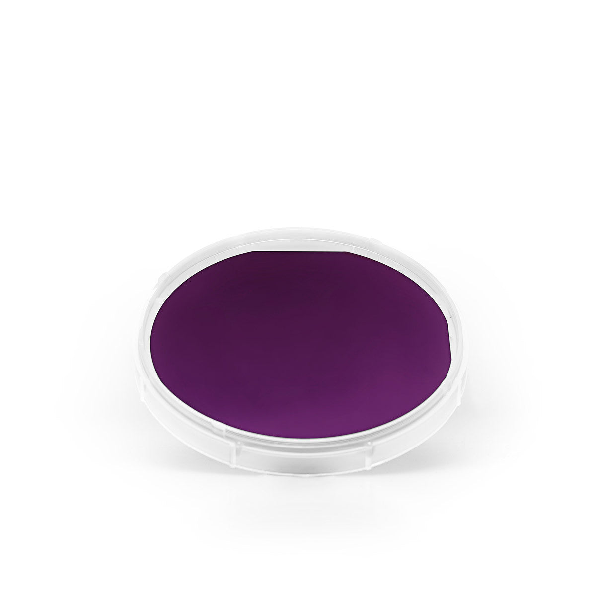


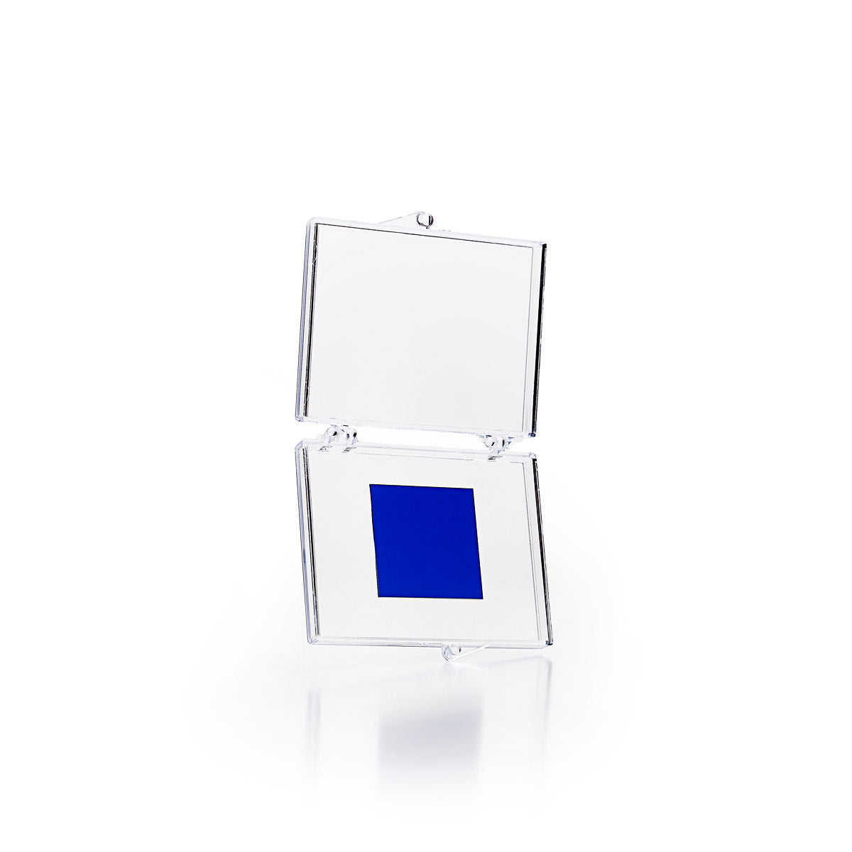


Monolayer Graphene on 300 nm SiO₂/Si - Fully Covered
Processed in ISO 7 Cleanroom
Our monolayer graphene on SiO₂/Si (fully covered) is a bidimensional material produced by CVD and transferred to a circular substrate of SiO₂/Si (300nm) by a semi-dry transfer process. We consider it to be a benchmark product in the graphene market - not only for its excellent quality, but also for its shape, size and number of applications.
Graphene Film
- · Growth method: CVD synthesis
- · Polymer assisted transfer
- · Appearance (color): Transparent
- · Transparency: > 97%
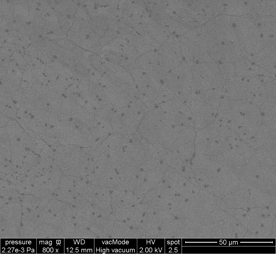
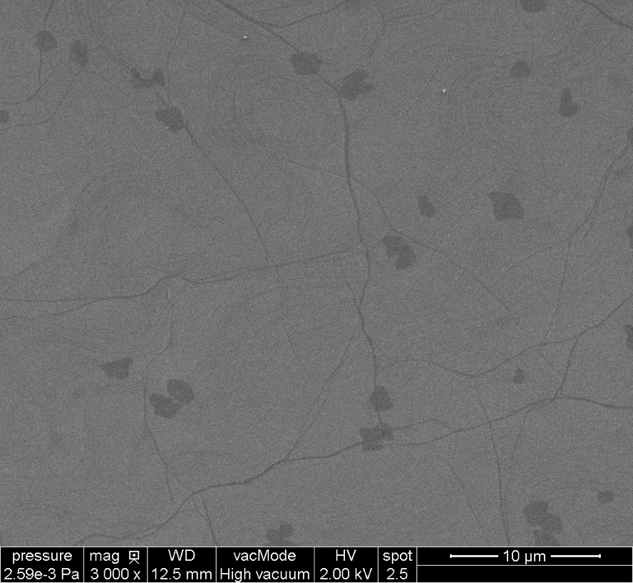
- · Coverage: > 95%
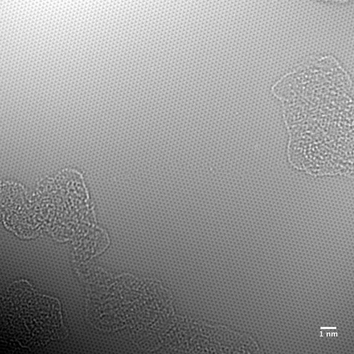
- · Number of graphene layers: 1
- · Thickness (theoretical): 0.345 nm
- · AFM Thickness (air @RT): <1nm
- · Electron Mobility on SiO2/Si: ≈1500 cm2/V·s
- · Sheet Resistance on SiO₂/Si: 350±40 Ohms/sq (1cm x1cm)
- · Grain size: Up to 20 μm
Substrate SiO₂/Si
- · Dry Oxide Thickness (both sides): 300 nm (+/-5%)
- · Type/Dopant: P/Bor
- · Resistivity: 1-10 ohm·cm
- · Thickness: 525 +/- 20 μm
- · Front surface: Polished
- · Dielectric Constant of the SiO2 layer: 3.9
Quality control
All our samples are subjected to a rigorous QC in order to ensure a high quality and reproducibility of the graphene. All our CVD materials are processed in ISO 7 Cleanroom. Each batch must pass the following tests:
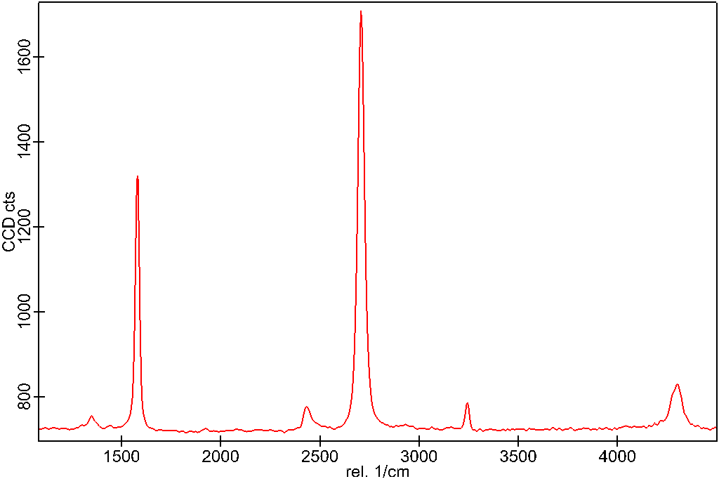
- · Raman Spectroscopy on each batch: I(G)/I(2D)<1; I(D)/I(G)<0.1 on 90nm SiO2/Si substrate.
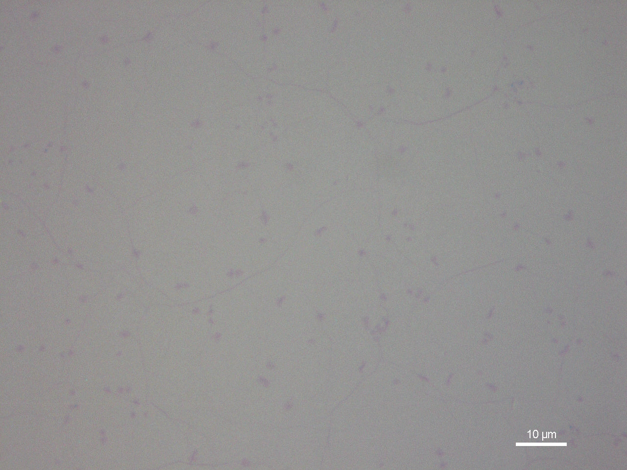
- · Optical Microscopy inspection of each individual sample to ensure good transfer quality and purity
If your application requires more specific controls (AFM, SEM...) please do not hesitate to contact us.
Applications
Graphene research, Graphene transistors and electronic applications, Graphene optoelectronics, plasmonics and nanophotonics, Graphene photodetectors (measure photon flux or optical power), Biosensors and bioelectronics, Aerospace industry (electronics, thermal interface materials, etc.), MEMS and NEMS
Publications
“Recent advances in graphene-based biosensors”
2011; doi: 10.1016/j.bios.2011.05.039.
“Optical nano-imaging of gate-tunable graphene plasmons”
Nature 487, 77-81 (05 July 2012), vol. 487, page 77, doi: 10.1038/nature11254
"Graphene Frequency Multipliers"
Electron Device Letters, IEEE, vol. 30, Issue:5; doi: 10.1109/LED.2009.2016443
 Data Sheet Graphene Film
  MSDS Graphene Film