A bandgap semiconductor nanostructure made entirely from graphene
In 2005, when Andre Geim and Philip Kim separately worked on graphene's electrons and showed that the material was showing a zero-bandgap, this came as a very curious feature that people would probably use. This zero-bandgap property makes that graphene is not a real semi-conductor and could not be used directly by the industry. Many successful attempts were made to create a band gap in graphene, by using doped graphene, nanoribbons or by using an electric field between a bi-layered graphene.
 Few would have thought about bending graphene to get a band gap. However, this idea has been followed by Edward Conrad since three years now in Georgia Tech. He has been working on graphene grown on surfaces with small grooves (18 nanometers deep). When graphene is deposited over these trenches a semiconducting behavior appears. The results were published this month in the journal Nature physics and show a 0.5 electonvolts band gap.
We asked Edward Conrad some questions about his last publication :
How did you get the idea to study graphene's conduction on a topological surface? Did you have any feelings about the result beforehand?
E. Conrad : Our group has been working on sidewall growth techniques for the last three years. The goal was to get around lithography defined ribbons that have very rough edges and therefore can not lead to semiconducting graphene. In the process developed at Georgia Tech we grow graphene on the walls of shallow trenches etched into Silicon carbide (SiC) that leads to very narrow ribbons. We have been developing arrays of these ribbons that are so well ordered that we can measure their electronic band structure using angle resolved photoemission. Our intent was to show directly that the graphene on the sidewalls was semiconducting.
After two years of work with no success, a wider set of data scans showed that the curved part of the the graphene, as it bends over the trench edge, becomes semiconducting. This was a big surprise to us! We did not expect the bend to have any significant gap. This is a classical example of how experimental physics runs down a path and finds a new turn in the road that was unexpected.
Has your research been inspired by some other previous work?
E. Conrad : We had no idea that this bent graphene would be such a good semiconductor. There has been theory work on strained graphene, but nothing I am aware suggest such a gap.
Can you give us some details about the growing of the graphene on your surface? Do you think that introducing trenches on the waffer can become critical in the deposition of graphene?
E. Conrad : Graphene grows ordered on Silicon Carbide. You heat the SiC in a carbon furnace and graphene grows. It has a specific orientation relative to the SiC atomic lattice. There was early work that showed graphene grows over atomic steps in SiC.
What we did was to patterned ordered arrays of steps in the SiC with know depth and orientation rather than rely on random steps that occur on the blank SiC wafers. The fact that graphene grows so ordered on SiC allowed us to make more than 10,000 parallel trenches and thus 10,000 graphene ribbons. This allowed us to have a system where we could measure the band structure of ribbons as small as 1.4nm wide.

Graphene grown on SiC trenches (left) - Photoemission spectroscopy (right)
Source : Nature Physics
Most people measure the band structure indirectly through resistance measurements. The problem with that method is that dirt, disorder, width variations all make the interpretation of these experiments difficult. Using our ordered system, we can measure the band structure, and therefore the gap, directly.
What are the direct applications you see in this result?
E. Conrad : Making high speed low power transistors out of graphene has always been the goal. Without a band gap this could never happen and graphene would never compete with Si transistors. We are currently trying to build a Schottky barrier transistor out of this material. If it works, it will open up a scalable way to make all carbon integrated circuits.
What could be industrial constraints about these applications?
E. Conrad : Thinking about industrial constraints at this point is a bad idea. First we must prove the device will work, then we worry about how to build them on an industrial scale. The example is the invention of the transistor. They built the first transistor out of germanium (Ge), one of the most expensive materials know at the time (only ~20 people ever held the stuff). When they found out Ge transistors did not work well enough they started a project to build it out of an even more expensive material that no one knew how to purify: silicon.
The point is, if the device has properties compelling enough the engineering will follow. In this case graphene can in principle operate at switching speeds much higher than silicon and does not have the same heating problems. If the device we are building works well enough, graphene high speed devices will start to enter the market.
How long have you been working on that project?
E. Conrad : I started working on graphene soon after the original patent for graphene electronics were submitted by Georgia Tech in 2001 (4 years before the work that led to a Nobel prize). By the way, the noble prize for graphene was given for its discovery in 2004 even though graphene was known to exist as early as 1960s and rediscovered again in the 1980s and 1990s.
What do you think about the media coverage about graphene?
E. Conrad : There is way too much media coverage. A lot of hype about future electronics when a band gap (step one in electronics) has never been shown to exist until now. There is a lot of serious work left to be done to prove that graphene electronics is feasible. Research is slow and methodical. People who make predictions should not always be listened too.
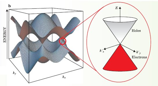
Graphene electronic diagram
Source : LPT Paris
If you want to follow news about graphene we suggest you to register to the mailing list and follow us on Twitter or Google+.
![]()
![]()
To know more : Hicks, J., Tejeda, A., Taleb-Ibrahimi, A., Nevius, M., Wang, F., Shepperd, K., Palmer, J., Bertran, F., Le Fèvre, P., Kunc, J., de Heer, W., Berger, C., & Conrad, E. (2012). A wide-bandgap metal–semiconductor–metal nanostructure made entirely from graphene Nature Physics DOI: 10.1038/nphys2487

