Electrical control of light emission near graphene
Controlling the energy emission of light sources is of fundamental interest and has many applications in photovoltaics, quantum optics, photodetection, biosensing, and other fields. In one of our most recent papers, team Graphenea together with collaborators from Spain, France, Italy, and the USA has demonstrated electrical control of the flow of light from an erbium light source near graphene.
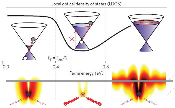
Image: Electrical control of light emission from erbium near graphene. Light is routed to free space, charge excitations in graphene, or plasmons in graphene, as graphene is switched from semiconductor to transparent material to metal.
Erbium nanocrystals are widely used in modern science as miniature sources of light. The crystals are small, with dimensions of several tens of nanometers, and emit light at a wavelength of 1530 nm, which is very convenient for optical communication. Erbium has been extensively tested for quantum optics, a branch of physics that focuses on utilizing the quantum states of photons for computation and communication. Quantum optics puts some tough requirements on the specific state of each photon, demanding extreme control of the properties of the emitted light.
On such a small scale, the direction, polarization, intensity, and rate of emission of emitted light strongly depend on where the emitter is located. A quantum light source near a fiber optic waveguide, for example, will preferentially emit into the fiber. The same source near a metal will, under certain conditions, not emit at all, a phenomenon known as ‘quenching’. In most studies to date, quantum emitters were placed in fixed engineered environments, without a particularly flexible way of tuning the emission. In our collaboration, our graphene has been used to actively modify with the turn of a knob the way erbium ions emit light.
The device presented in the paper entitled “Electrical control of optical emitter relaxation pathways enabled by graphene”, published January 2015 in Nature Physics, consists of a graphene layer on top of an erbium-doped substrate material. The graphene is capped with a polymer electrolyte, which enables strong doping of the graphene. The high level of doping with this method allows us to sweep the Fermi energy from nearly zero all the way up to nearly 1 eV, during which sweep the graphene goes from semiconductor to transparent material to metal. The changing properties of nearby graphene force the erbium to redirect light from free space to carrier excitations in the graphene sheet, and finally to plasmons in graphene. This unique ability to electrically tune the dielectric environment of a nano-emitter opens up avenues in a range of fields, both fundamentally and on the application level.
Graphenea provided the graphene for the experiment. The rest of the materials came from Italy and France, whereas the actual experiments were carried out in collaboration between ICFO near Barcelona and the Massachusetts Institute of Technology.
This is our third paper in the Nature family of journals, all of which are the result of the extremely fruitful collaboration that Graphenea has with Prof. Frank Koppens at ICFO. We strive to continue our strong presence in the scientific research community through collaborations with world-leading graphene scientists.

